-
English
-
English 
STEREO by C.P.U. (2006) , Robert Petružela (Bob!k) & Radek Štěrba (Raster)
4-6-2007 - Updated description, added photos.
27-6-2007 - Translated by Pepax. (Thanks!)
|
Important notice: If you decide to make a stereo upgrade according to the following schematics and instructions you do it at your own risk! The authors' intention was to create preferably the least invasive solution without irreversible changes to the Atari computer and damaging the Pokey chips by bending their pins. (Some brutal howtos even suggest cutting the unused pins off - please don't ever do that!) If you decide to somehow modify your Atari please do it carefully and avoid any unnecessary alternation. Atari XE stereo
upgrade description: |
|
|
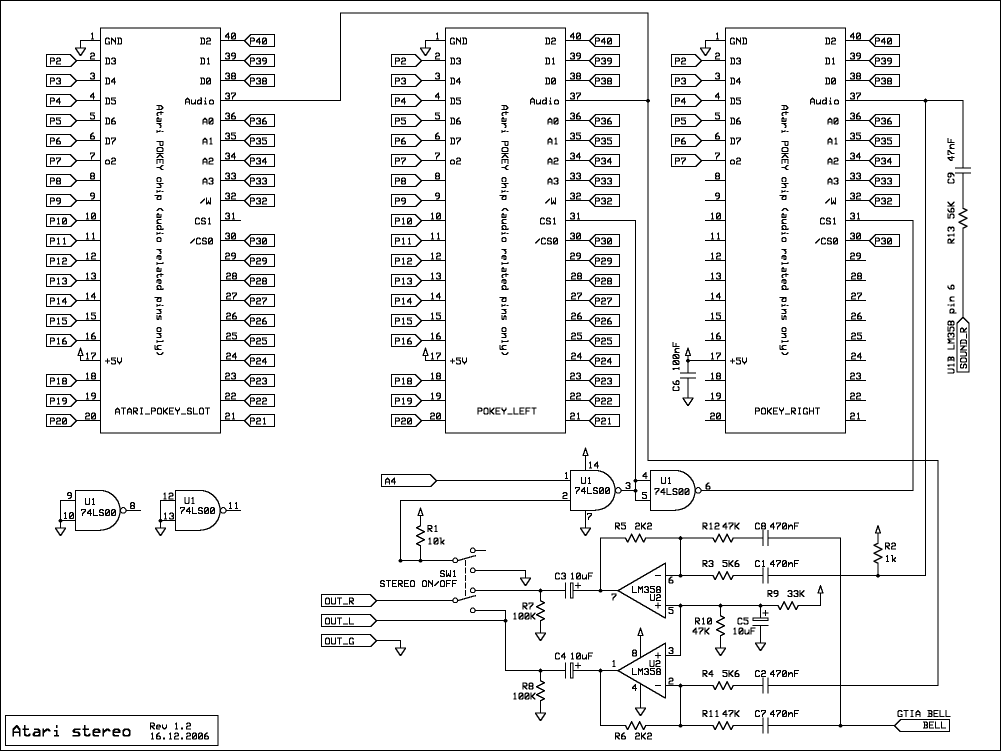
Schematics: |
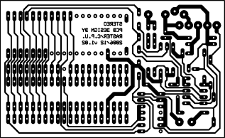
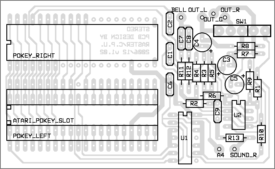
PCB layout: |
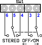
| Parts: ATARI_POKEY_SLOT ... DIL40 double sided pins (2 x 20 pins) POKEY_LEFT ... DIL40 precision socket + Atari POKEY chip POKEY_RIGHT ... DIL40 precision socket + Atari POKEY chip SW1 ... 2 pole 2 position switch C1,C2,C7,C8 ... 470nF C3,C4,C5 ... 10uF C6 ... 100nF C9 ... 47nF R1 ... 10K R2 ... 1K R3,R4 ... 5K6 R5,R6 ... 2K2 R7,R8 ... 100K R9 ... 33K R10,R11,R12 ... 47K R13 ... 56K U1 ... 74LS00 U2 ... LM358 Note: Don't forget to buy an additional DIL40 precision socket that will replace the Pokey chip on the motherboard, in which one side of the double sided DIL40 pins on the stereo PCB will be inserted. The solder side of the PCB holds the double sided DIL40 pins only. It is necessary to file down their plastic sides to bare the pins partially to be able to solder them in place. All other parts are located on the component side. Solder the double sided pins last, not to prevent yourself from soldering the POKEY_LEFT precision socket. Insert the Pokeys only after finishing all the soldering. |
PCB layout with silkscreen layer: |
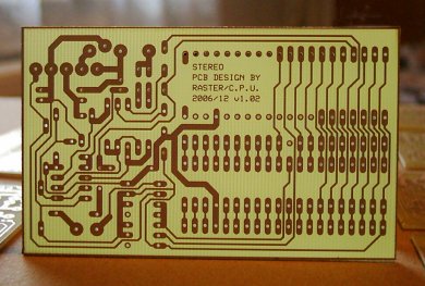 Photo of the PCB - solder side. |
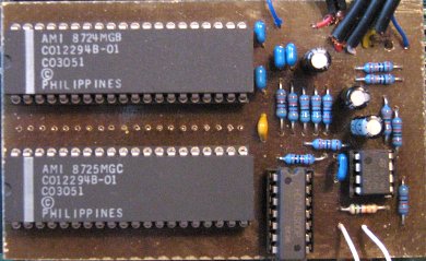 Photo of the populated PCB. (View of the upper - component side.) |
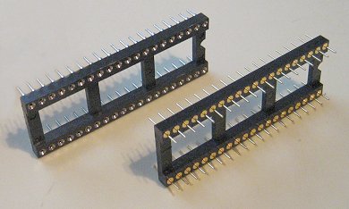 Parts: DIL40 precision socket on the left, double sided DIL40 pins on the right. |
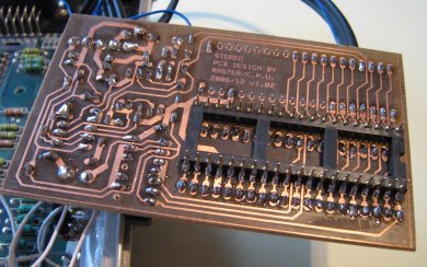 The lower - solder side of the PCB. It is necessary to file off the plastic sides of the double sided pins for soldering. |
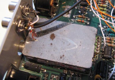 Audio out cinch connectors nicely fit above the TV modulator. See the U1B (LM358) chip right of the modulator. The SOUND_R signal from the stereo PCB is connected to its pin #6 with the white wire. (Note: the other white and orange wires in the top right corner are unrelated to the stereo upgrade.) |
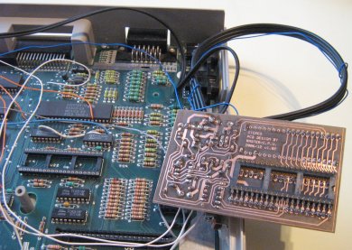 Atari with the precision socket soldered in. The stereo upgrade PCB snaps in and can be replaced with the original Pokey chip any time (after desoldering the wires). |
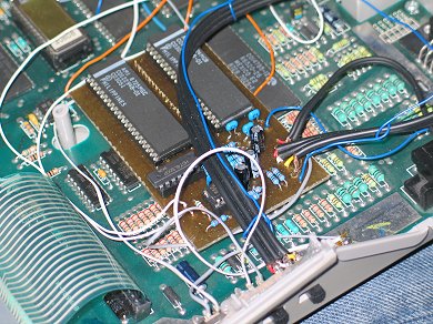 Overall view of the PCB in place. The three black shielded wires, along with the blue one, head to the side of the Atari where the mono/stereo switch is mounted. The black shielded double wire leads to the audio out cinch connectors. The other blue wire carries the BELL signal from GTIA. The two white wires on the opposite side carry the A4 and SOUND_R signals. (Note: The other wires and switches on Atari's side are unrelated to the stereo upgrade PCB. In this case they are parts of the RAM and OS upgrades.) |
|